FPGA Transceiver
Transceiver
This block provides a level of abstraction between the precise CP2200/1 interface and a generalized interface seen by the internal blocks of the FPGA. This eliminates a need for the internal workings of the FPGA to be aware of the timing of the interface; they simply order a start of transfer and wait for notification of the transfer's completion. The transceiver for its part initiates a read or write conversation with the CP2200/1 over the multiplex Intel bus upon request from the internals and returns data, if applicable, along with a "Done" pulse at the end of the conversation.
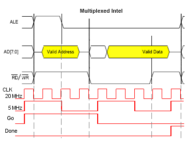
This unit serves as a bridge between the Ethernet Controller chip and the FPGA in terms of timing as well. The latter is run at the rate of its slowest client: the Temperature sensor which has a top recommended clock rate of 10 MHz. Given that CP2200/1 prefers 20 MHz, it was resolved that the FPGA will run on a 5 MHz clock subdivided from the Ethernet Controller's. The transceiver performs this subdivision and ensures data latching on the external and internal buses, as shown in the adjacent diagram.
Programming Details
Clock subdivision from 20 MHz to 5 MHz is done in a straightforward with a counter.
The timing of the Muxed Intel bus conversation with the EC is nicely metered out by the 20 MHz clock. Each half-wave of the fast clock is 25 ns, which turns out to be a convenient multiple with which to count off the required waiting periods. The module has been written carefully to satisfy the timing requirements outlined in the EC manual. As seen in the figure, the entire conversation turns out to take only two slow clock cycles, making the delay for the FPGA internals negligible.
Ports
- Clk: [in] clock
- Rst: [in] asynchronous reset
- fClk: [in] "fast" - 20 MHz board clock
- Clk: [out] "slow" - subdivided 5 MHz internal FPGA clock (satisfies Temp. sensor's <10 MHz requirement)
- Rst: [in] asynchronous reset
Multiplexed Intel bus lines - EC interface
- ALE: [out] conversation-start flag
- AD : [inout] two-way 8-bit address and data bus
- iRD: [out] active-low read flag
- iWR: [out] active-low write flag
FPGA-Internal input lines
- TxRx_Go: [in] "Go" signal to read/write an EC control register byte
- TxRx_RiW: [in] active-high read, active-low write flag
- TxRx_Ain: [in] 8-bit address of EC control register
- TxRx_Din: [in] 8-bit write data for EC control register
- TxRx_Dout: [out] 8-bit data bus carrying returned value from EC
- TxRx_Done: [out] "Done" signal
