SiPM digital control board
The SiPM digital control board provides remote control and monitoring of the SiPM (silicon photomultiplier) electronics. Variation in performance from one SiPM to the next, their temperature sensitivity, variation from one optical channel to the next as well as varying output due to scintillator degradation from radiation calls for active control of individual SiPMs to compensate for adverse effects.
Responsibilities of the control board
The control board is responsible for providing a layer of interaction between the researchers running the experiments and the tagger microscope's SiPM electronics. The foremost responsibility of the control board is to allow the users to program the SiPM bias voltage, which controls the gain and photo-detection efficiency. It receives signals from an external PC and communicates that information to a DAC which controls the bias voltage. It also monitors itself and reports back to the PC certain statistics, such as voltage of the power lines (to ensure the chips and SiPMs are receiving the required voltages) and temperature of the control and amplifier boards (to ensure that the electronics are not overheating). Additionally, voltage information read back from the DAC allows for feedback that assists calibration.
The Components
The hub of the control board, its "central nervous system", is an FPGA. All components on the board connect to the FPGA and it coordinates their interactions. Communication with the outside world (more specifically an external PC) occurs over Ethernet. This was a natural choice, being a robust, long distance, inexpensive communication bus. To implement this, an Ethernet controller chip is included on the board and connected to the FPGA. There are two monitoring devices so that the board can ensure that it is running properly: a temperature sensor and an ADC.
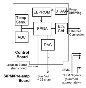
The adjacent diagram shows the component connection scheme. The dashed horizontal line represents the "backplane" board which interfaces the digital control board with the SiPM amplifier board and seals the latter inside the light-tight microscope enclosure while keeping the control board outside for easy cable connection. As shown, up to 32 voltage lines on the amplifier board may be controlled by the DAC chip chosen of the control board design. In practice, the natural segmentation of the optical channels makes 25 or 30 channels the maximum. Conveniently, the remaining 2 DAC channels are used for amplifier gain selection and for calibration. It is important to note that the Ethernet based control board is not addressed only by its MAC address, but is automatically cross-referenced to its location in the microscope electronics board array. An "Location Stamp" number, jumper-coded into the backplane slot to which the control board is connected clarifies its identity in terms of the microscope energy bins it controls. This significantly simplifies setup, since a once time slot-coding fixes the board address space no matter which generic copy of the control board is inserted.
A detailed representation of the component interconnected is provided in the SiPM digital control board netlist. Additionally, more detailed information on the supporting components is available.
The FPGA
The FPGA is the hub of the digital control board. All components communicate through the FPGA and are controlled by the FPGA. The chip we plan to use is the Xilinx Spartan-3A FPGA. The Spartan line of FPGAs are low-cost chips well-suited for small designs such as this. The 3A model is optimized for I/O and includes a large number of I/O pins, which will be beneficial considering the amount of interconnect relative to the amount of logic. The code for the FPGA, written in VHDL, is complete. Remaining tweaks are subject to the use experience during beam tests and any other field experience. The code fits within the smallest version of the chip in terms of gates and pins, which greatly simplifies the board assembly and reduces cost. The design did, however rely on Xilinx primitives (instantiation of device-specific resources) for large registers required by the code.
The data sheet, user guide, configuration guide, and other documentation regarding the FPGA can be downloaded from the Xilinx website.
Much of the FPGA programming is concerned with the complex operations of the Ethernet controller chip CP2200/1 discussed below. This core interacts with the DAC and the SPI-based ADC and Temperature sensor when access to these chips is required. Please see the relevant pages from the following list.
- Programming the Ethernet controller (core of FPGA design)
- Reset and Initialization - discussion of reset/initialization needs of our chips.
- Programming the DAC controller
The Ethernet controller
After researching a variety of communication buses, including USB, I2C, FireWire, and various others, it was decided that the best choice would be Ethernet. Ethernet is based on a multi-layer protocol, with each higher layer adding more advanced capabilities. Only layers one and two are necessary for our purposes, being a local network not connected to a true internet. In addition, due to the wide availability of Ethernet hubs/switches, Ethernet will help to minimize the number of wires that must be run between the control board array and the main computer.
We have selected the Silicon Laboratories CP2200/1 Ethernet controller. The two variants of the chip differ (primarily) in packaging and I/O pin count: the CP2201 requires a Multiplexed Intel Bus interface, saving many pins. The FPGA has been designed around this chip.
The data sheet and other information regarding the Ethernet controller can be downloaded from the Silicon Laboratories website.
The DAC
The purpose of the control board is to allow remotely programmable bias voltages for the SiPMs. For this purpose a DAC is required. The current design of the tagger microscope calls for 16 SiPMs per electronics card, however designs of up to 24 SiPMs per electronics card are being considered. Various designs were studied, but based on availability of components in the 50V range (DACs and op-amps primarily) the most suitable choice found was the Analog Devices' AD5535. It can go up to 200V with a resolution of 14 bit (roughly 12mV at 200V scale, roughly 3mV at a 50V scale) on 32 channels. As there are so many channels built in to this system, the tagger may be slightly restructured so as to include up to 32 SiPMs per board instead of 16 per board. This DAC defines its own serial interface for communication with the FPGA.
The data sheet and other information regarding the DAC can be downloaded from the Analog Devices website.
The ADC
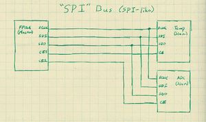
In order to monitor the voltage levels of the power lines and possibly some DAC channels, an ADC is to be included in the design. The Analog Devices' AD7928 is an eight-channel ADC. Based on the selection of components there are six necessary power lines and two necessary grounds, so the AD7928 is capable of monitoring the entire system if need be. It uses a serial protocol that is compatible with the SPI bus to communicate with the FPGA.
The data sheet and other information regarding the ADC can be downloaded from the Analog Devices website.
Temperature sensor
In order to monitor the ambient temperature, a temperature sensor is to be included in the design. The Analog Devices' AD7314 has ten-bit resolution on temperature and is compatible with the SPI bus for communication with the FPGA.
The data sheet and other information regarding the temperature sensor can be downloaded from the Analog Devices website.
Important Links
Here is a summary of important pages relating to the SiPM digital control board instrumentation.


