Programming the FPGA
The FPGA is the hub of the digital control board and all other chips are connected to and controlled by it. This article discusses the programming of the FPGA. All code is written in VHDL. For the purposes of testing, each chip has not only a controller written for it, but an emulator as well.
The DAC
Interface
The AD5535 Digital-to-Analog Converter has a three-wire serial interface and an inverted-logic reset signal. A serial communication transfers one 19-bit word:
| ||||||||||||||||||||||||||||||||||||||
- A(4:0) is a 5-bit address to select the target DAC channel. A4 is the most-significant bit and transfers first.
- DB(13:0) is a 14-bit voltage code, where .
- DB = 0 yields .
- DB = (full scale) yields .
The three lines of the interface are SYNC, SCLK, and D_in. A write to the DAC begins with a falling edge of SYNC. The next 19 bits (counted off by SCLK) are saved into a shift register The next transfer begins on another falling edge of SYNC, but transfers do not overlap or interrupt. A minimum of 200ns is required between exchanges. SCLK is ignored except during the 19 shift cycles. The minimum clock pulse width is 13ns high and 13ns low, yielding a maximum frequency of 77MHz theoretically. In actual fact the maximum clock frequency is 30MHz and the maximum word frequency is 1.2MHz. For further details on timing and protocol, see the AD5535 data sheet supplied by Analog Devices, in particular "Timing Characteristics" (p.5) and "Functional Description (p.12).
Emulator
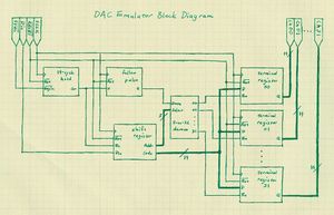
The functional block diagram for the emulator is shown to the right. The blocks are:
- 19-cycle hold
- This block takes the single input pulse (one clock cycle wide) and generates a 19-cycle-wide pulse to tell the shift register how long to read in new data. It ignores any additional pulses while the 19-cycle pulse is running. It also enforces a gap of one cycle between serial words.
- inputs: asynchronous, active-low reset; clock; active-low input pulse
- outputs: 19-cycle pulse
- shift register
- This is a serial-in, parallel-out, 19-bit shift register. While the enable line is high it clocks in data. The output is nominally partitioned between address and code, but this is implemented not inside the shift register but by routing the output lines appropriately.
- inputs: asynchronous, active-low reset; data-in serial line; enable; clock
- outputs: 5-bit parallel address bus; 14-bit parallel code bus
- follow pulse


