Difference between revisions of "Programming the FPGA"
| Line 7: | Line 7: | ||
== The DAC == | == The DAC == | ||
| − | + | === DAC interface === | |
| − | = | ||
The AD5535 Digital-to-Analog Converter has a three-wire serial interface and an inverted-logic reset signal. A serial communication transfers one 19-bit word: | The AD5535 Digital-to-Analog Converter has a three-wire serial interface and an inverted-logic reset signal. A serial communication transfers one 19-bit word: | ||
| Line 29: | Line 28: | ||
The three lines of the interface are ''SYNC'', ''SCLK'', and ''D_in''. A write to the DAC begins with a falling edge of ''SYNC''. The next 19 bits (counted off by ''SCLK'') are saved into a shift register The next transfer begins on another falling edge of ''SYNC'', but transfers do not overlap or interrupt. A minimum of 200ns is required between exchanges. ''SCLK'' is ignored except during the 19 shift cycles. The minimum clock pulse width is 13ns high and 13ns low, yielding a maximum frequency of 77MHz theoretically. In actual fact the maximum clock frequency is 30MHz and the maximum word frequency is 1.2MHz. For further details on timing and protocol, see the AD5535 data sheet supplied by Analog Devices, in particular "Timing Characteristics" (p.5) and "Functional Description (p.12). | The three lines of the interface are ''SYNC'', ''SCLK'', and ''D_in''. A write to the DAC begins with a falling edge of ''SYNC''. The next 19 bits (counted off by ''SCLK'') are saved into a shift register The next transfer begins on another falling edge of ''SYNC'', but transfers do not overlap or interrupt. A minimum of 200ns is required between exchanges. ''SCLK'' is ignored except during the 19 shift cycles. The minimum clock pulse width is 13ns high and 13ns low, yielding a maximum frequency of 77MHz theoretically. In actual fact the maximum clock frequency is 30MHz and the maximum word frequency is 1.2MHz. For further details on timing and protocol, see the AD5535 data sheet supplied by Analog Devices, in particular "Timing Characteristics" (p.5) and "Functional Description (p.12). | ||
| − | + | === DAC emulator === | |
| − | = | ||
[[Image:DAC Emulator Block.JPG|thumb|DAC emulator functional block diagram]] | [[Image:DAC Emulator Block.JPG|thumb|DAC emulator functional block diagram]] | ||
| Line 78: | Line 76: | ||
*** ''Q'': 14-bit output bus | *** ''Q'': 14-bit output bus | ||
| − | + | === DAC controller === | |
| − | = | ||
[[Image:DAC Controller Block.JPG|thumb|DAC controller functional block diagram]] | [[Image:DAC Controller Block.JPG|thumb|DAC controller functional block diagram]] | ||
| Line 106: | Line 103: | ||
== The temperature sensor == | == The temperature sensor == | ||
| − | + | === Temperature sensor interface === | |
| − | = | ||
The AD7314 temperature sensor uses a four-wire interface related to (and compatible with) the [http://en.wikipedia.org/wiki/Serial_Peripheral_Interface_Bus SPI bus] protocol. The wires are: | The AD7314 temperature sensor uses a four-wire interface related to (and compatible with) the [http://en.wikipedia.org/wiki/Serial_Peripheral_Interface_Bus SPI bus] protocol. The wires are: | ||
| Line 120: | Line 116: | ||
A read operation occurs during a 16-cycle pulse of ''CE''. The first transmitted bit will be zero, followed by ten bits of temperature data (MSB first). The remaining five bits are copies of the final data bit. After ''CE'' goes low ''SDO'' goes into a high-Z state. Temperature data is given in degrees Celsius. The format is two's-complement with two decimal places; in essence it is standard two's-complement, then the result must be divide by four after converting to decimal. | A read operation occurs during a 16-cycle pulse of ''CE''. The first transmitted bit will be zero, followed by ten bits of temperature data (MSB first). The remaining five bits are copies of the final data bit. After ''CE'' goes low ''SDO'' goes into a high-Z state. Temperature data is given in degrees Celsius. The format is two's-complement with two decimal places; in essence it is standard two's-complement, then the result must be divide by four after converting to decimal. | ||
| − | + | === Temperature sensor emulator === | |
| − | = | ||
[[Image:Temp Emulator Block.JPG|thumb|Temperature sensor emulator functional block diagram]] | [[Image:Temp Emulator Block.JPG|thumb|Temperature sensor emulator functional block diagram]] | ||
| Line 144: | Line 139: | ||
*** ''Ser'': serial output line | *** ''Ser'': serial output line | ||
| − | + | === Temperature sensor controller === | |
| − | = | ||
[[Image:Temp Controller Block.JPG|thumb|Temperature sensor controller functional block diagram]] | [[Image:Temp Controller Block.JPG|thumb|Temperature sensor controller functional block diagram]] | ||
Revision as of 21:51, 5 July 2007
The FPGA is the hub of the digital control board and all other chips are connected to and controlled by it. This article discusses the programming of the FPGA. All code is written in VHDL. For the purposes of testing, each chip has not only a controller written for it, but an emulator as well.
Open questions
What is the clock speed of the FPGA? Timing constraints must be taken into account to link the multiple blocks.
The DAC
DAC interface
The AD5535 Digital-to-Analog Converter has a three-wire serial interface and an inverted-logic reset signal. A serial communication transfers one 19-bit word:
| ||||||||||||||||||||||||||||||||||||||
- A(4:0) is a 5-bit address to select the target DAC channel. A4 is the most-significant bit and transfers first.
- DB(13:0) is a 14-bit voltage code, where .
- DB = 0 yields .
- DB = (full scale) yields .
The three lines of the interface are SYNC, SCLK, and D_in. A write to the DAC begins with a falling edge of SYNC. The next 19 bits (counted off by SCLK) are saved into a shift register The next transfer begins on another falling edge of SYNC, but transfers do not overlap or interrupt. A minimum of 200ns is required between exchanges. SCLK is ignored except during the 19 shift cycles. The minimum clock pulse width is 13ns high and 13ns low, yielding a maximum frequency of 77MHz theoretically. In actual fact the maximum clock frequency is 30MHz and the maximum word frequency is 1.2MHz. For further details on timing and protocol, see the AD5535 data sheet supplied by Analog Devices, in particular "Timing Characteristics" (p.5) and "Functional Description (p.12).
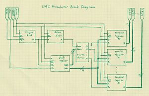
DAC emulator
The functional block diagram for the emulator is shown to the right. The blocks are:
- 19-cycle hold
- This block takes the single input pulse (one clock cycle wide) and generates a 19-cycle-wide pulse to tell the shift register how long to read in new data. It ignores any additional pulses while the 19-cycle pulse is running. It also enforces a gap of one cycle between serial words.
- inputs
- Reset: asynchronous, active-low reset
- CLK: clock
- Begin: active-low input pulse
- outputs
- Go: 19-cycle pulse
- shift register
- This is a serial-in, parallel-out, 19-bit shift register. While the enable line is high it clocks in data. The output is nominally partitioned between address and code, but this is implemented not inside the shift register but by routing the output lines appropriately.
- inputs
- Reset: asynchronous, active-low reset
- D_in: data-in serial line
- En: enable
- Clk: clock
- outputs
- Addr: 5-bit parallel address bus
- Code: 14-bit parallel code bus
- follow pulse
- This block monitors the enable line generated by the 19-cycle hold block. At the end of the pulse it sees a falling edge and sends a single-cycle pulse to notify the terminal registers that the shift register has loaded a complete word and is ready to write.
- inputs
- Reset: asynchronous, active-low reset
- Clk: clock
- D: 19-cycle input pulse
- outputs
- Q: single-cycle following pulse
- 5-to-32 demux
- This block is a 5-to-32 demultiplexer. It uses the address generated by the shift register to direct the read-enable pulse from the follow pulse block to the appropriate terminal register.
- inputs
- Select: 5-bit-wide select bus
- Data: data line
- outputs
- 00:31: 32 enable lines (on per terminal register)
- terminal register (x32)
- This is a 14-bit, parallel-in, parallel-out register. There is one terminal register for every channel.
- inputs
- Reset: asynchronous, active-low reset
- Clk: clock
- D: 14-bit data bus
- En: read enable
- outputs
- Q: 14-bit output bus
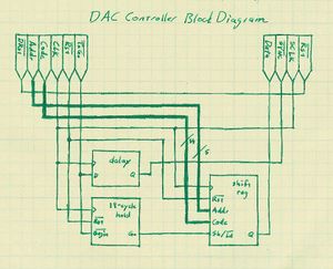
DAC controller
The functional block diagram for the controller is shown to the right. The blocks are:
- 19-cycle hold
- Identical to the component of the same name in the DAC emulator (see above)
- delay
- Delays all signals by one clock cycle
- inputs
- Clk: clock
- D: signal in
- outputs
- Q: signal out
- shift register
- A 19-bit, parallel-in, serial-out shift register. It reads in values every clock cycle that Sh/Rd is low and shifts out values every clock cycle that Sh/Rd is high. The signal is MSB of Addr to LSB of Code.
- inputs
- Clk: clock
- Reset: asynchronous, active-low reset
- Addr: 5-bit address bus
- Code: 14-bit code bus
- Sh/Ld: positive-logic shift/negative-logic load
- outputs
- Q: serial out line
The temperature sensor
Temperature sensor interface
The AD7314 temperature sensor uses a four-wire interface related to (and compatible with) the SPI bus protocol. The wires are:
- CE: Chip Enable (input), positive logic enable for SCLK
- SCLK: Serial Clock (input), clock line supplied by external source
- SDI: Serial Data In (input), data input line
- SDO: Serial Data Out (output), data output line
Note that the input/output notations are for slave devices (such as the temperature sensor) but are reversed for master devices (such as the FPGA). Proper SPI protocol flips the I/O polarity of CE and SCLK and crosses the SDI and SDO lines so that SDI is an input on every device and SDO is always an output. To maintain simplicity in wiring conventions we are not using proper SPI protocol, but are calling the slave input/master output line SDI and the slave output/master input line SDO so that the SDI/O notations are proper for slaves. The maximum clock rate is no higher than 10MHz. The interface, having separate input and output lines, is full-duplex; in fact the temperature sensor is unable to function in half-duplex mode. Outputs from the temperature sensor change on rising edges of SCLK, but inputs are latched on falling edges.
There is only one write operation to the temperature sensor and that is used to direct the temperature sensor to enter power-down mode. We do not plan to use this mode, so the SDI input on the temperature sensor will be tied to ground.
A read operation occurs during a 16-cycle pulse of CE. The first transmitted bit will be zero, followed by ten bits of temperature data (MSB first). The remaining five bits are copies of the final data bit. After CE goes low SDO goes into a high-Z state. Temperature data is given in degrees Celsius. The format is two's-complement with two decimal places; in essence it is standard two's-complement, then the result must be divide by four after converting to decimal.
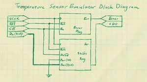
Temperature sensor emulator
The functional block diagram for the emulator is shown to the right. The blocks are:
- Error Flag
- The error flag goes high if the enable line is high for 1-15 or 17+ cycles. It resets to low any time the enable line goes back to high. It is used to notify of a "bad" transmission (not 16 cycles long).
- inputs
- Clk: clock
- Rst: asynchronous, active-low reset
- En: enable
- outputs
- Err: error flag
- Shift Reg
- An 11-bit, parallel-in, serial-out shift register that loads when not shifting.
- inputs
- Clk: clock
- Rst: asynchronous, active-low reset
- Sh/Ld: active-high shift, active-low load
- Par(10:0): 11-bit parallel input bus
- outputs
- Ser: serial output line
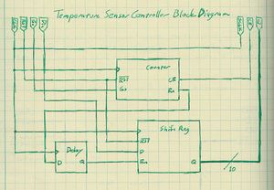
Temperature sensor controller
The functional block diagram for the controller is shown to the right. The blocks are:
- Counter
- Counts a cycle of 17 pulses; holds En high for 11 pulses, holds CE high for 16 pulses.
- inputs
- Clk: clock
- Rst: asynchronous, active-low rest
- Go: trigger to begin cycle
- outputs
- CE: serial chip enable
- En: internal shift enable
- Delay
- Delays input by one clock cycle.
- inputs
- Clk: clock
- D: input signal
- outputs
- Q: output signal
- Shift Reg
- A 10-bit, serial-in, parallel-out shift register.
- inputs
- Clk: clock
- Rst: asynchronous, active-low rest
- D: input signal
- En: shift enable
- outputs
- Q: 10-bit output bus


